Lattice ICE40
These circuits are the low-level primitives for the Lattice ICE40 FPGAs,
originally designed by Silicon Blue (hence, the prefix SB_).
Detailed documentation on these primitives is available in the Lattice iCE Technology Library and the Lattice iCE40 LP/HX Family Datasheet.
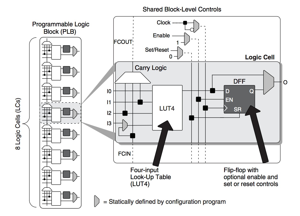
Programmable Logic Block
The programmable logic block consists of a vertical column of 8 logic cells. Each logic cell containts three components, a 4-bit lookup table (LUT4), a Carry unit, and a D-flip-flop (DFF)..
LUTS
The combinational logic primitive is a 4-bit LUT.
# SB_LUT4 :: I0:In(Bit), I1:In(Bit), I2:In(Bit), I3:In(Bit), O:Out(Bit)
SB_LUT4(LUT_INIT=int16))
The LUT is initialized by setting the parameter INIT to a 16-bit integer value. The output for a given input is equal to the bit at the position corresponding to the input value.
Carry
# SB_CARRY() :: I0:In(Bit), I1:In(Bit), CI:In(Bit), CO:Out(Bit)
SB_CARRY()
This functional unit computes the carry out given 3 inputs, including the carry in which must come from the previous logic cell in the vertical column.
CO = (I0&I1)|(I1&CI)|(CI&I0)
Flip-Flops
The ice40 DFF flip-flop can be configured in many different ways.
SB_DFF(init=0, has_ce=False, has_reset=False, has_set=False, edge=True, sync=True)
The input can be stored in the flip-flop on the rising (edge=True) or falling (edge=False) edge. The flip-flop can optionally contain a clock enable. The flip-flop can be configured to have a reset or set input, but not both. The reset and set can be configured to be either synchronous (sync=True) or asynchroous (sync=False). The DFFs are always initialized to 0.
# DFF w/ Clock enable
SB_DFFE() :: C:In(Bit), E:In(Bit), D:In(Bit), Q:Out(Bit)
# DFF w/ Synchronous Reset
SB_DFFSR() :: C:In(Bit), R:In(Bit), D:In(Bit), Q:Out(Bit)
# DFF w/ Asynchronous Reset
SB_DFFR() :: C:In(Bit), R:In(Bit), D:In(Bit), Q:Out(Bit)
# DFF w/ Synchronous Set
SB_DFFSS() :: C:In(Bit), S:In(Bit), D:In(Bit), Q:Out(Bit)
# DFF w/ Asynchronous Set
SB_DFFS() :: C:In(Bit), S:In(Bit), D:In(Bit), Q:Out(Bit)
# DFF w/ Synchronous Reset, Clock enable
SB_DFFESR() :: C:In(Bit), E:In(Bit), R:In(Bit), D:In(Bit), Q:Out(Bit)
# DFF w/ Asynchronous Reset, Clock enable
SB_DFFER() :: C:In(Bit), E:In(Bit), R:In(Bit), D:In(Bit), Q:Out(Bit)
# DFF w/ Synchronous Set, Clock enable
SB_DFFESS() :: C:In(Bit), E:In(Bit), S:In(Bit), D:In(Bit), Q:Out(Bit)
# DFF w/ Asynchronous Set, Clock enable
SB_DFFES() :: C:In(Bit), E:In(Bit), S:In(Bit), D:In(Bit), Q:Out(Bit)
Memory
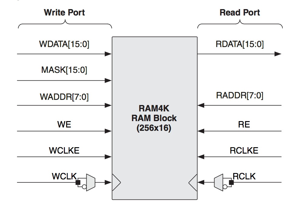
The memory blocks on the ice40 are 4 kilo-bits, and instanced using the following function.
# SB_RAM40_4K() ::
#    RDATA:Out(Bits(16)), # Read Data
#    RADDR:In(Bits(11)),  # Read Address
#    RCLK:In(Bit),        # Read Clock
#    RCLKE:In(Bit),       # Read Clock Enable
#    RE:In(Bit),          # Read Enable
#    WCLK:In(Bit),        # Write Clock
#    WCLKE:In(Bit),       # Write Clock Enable
#    WE:In(Bit),          # Write Enable
#    WADDR:In(Bits(11)),  # Write Address
#    MASK:In(Bits(16)),   # Write Mask
#    WDATA:In(Bits(16))   # Write Data
SB_RAM40_4K() ::
There is a utility function RAMB which configures the memory as a RAM, and
another ROMB that configures it as a ROM. This memory is initialized with
the contents of rom (for ROMB) or ram (for RAMB). The aspect ratio
(height x width) of the memory depends on the length of the array rom or
ram.
The following aspect ratios are allowed:
2048x2,
1024x4,
512x8,
256x16.
# RADDR: In(Bits(height),
# RDATA, In(Bits(width),
# RCLK,  In(Bit),
# RCLKE, In(Bit),
# RE,    In(Bit)
# WADDR: In(Bits(height),
# WDATA, In(Bits(width),
# WCLK,  In(Bit),
# WCLKE, In(Bit),
# WE,    In(Bit)
ROMB(height, width, ram=None):
# RADDR: In(Bits(height),
# RDATA, In(Bits(width),
# RCLK,  In(Bit),
# RCLKE, In(Bit),
# RE,    In(Bit)
ROMB(height, width, rom=None):
IO
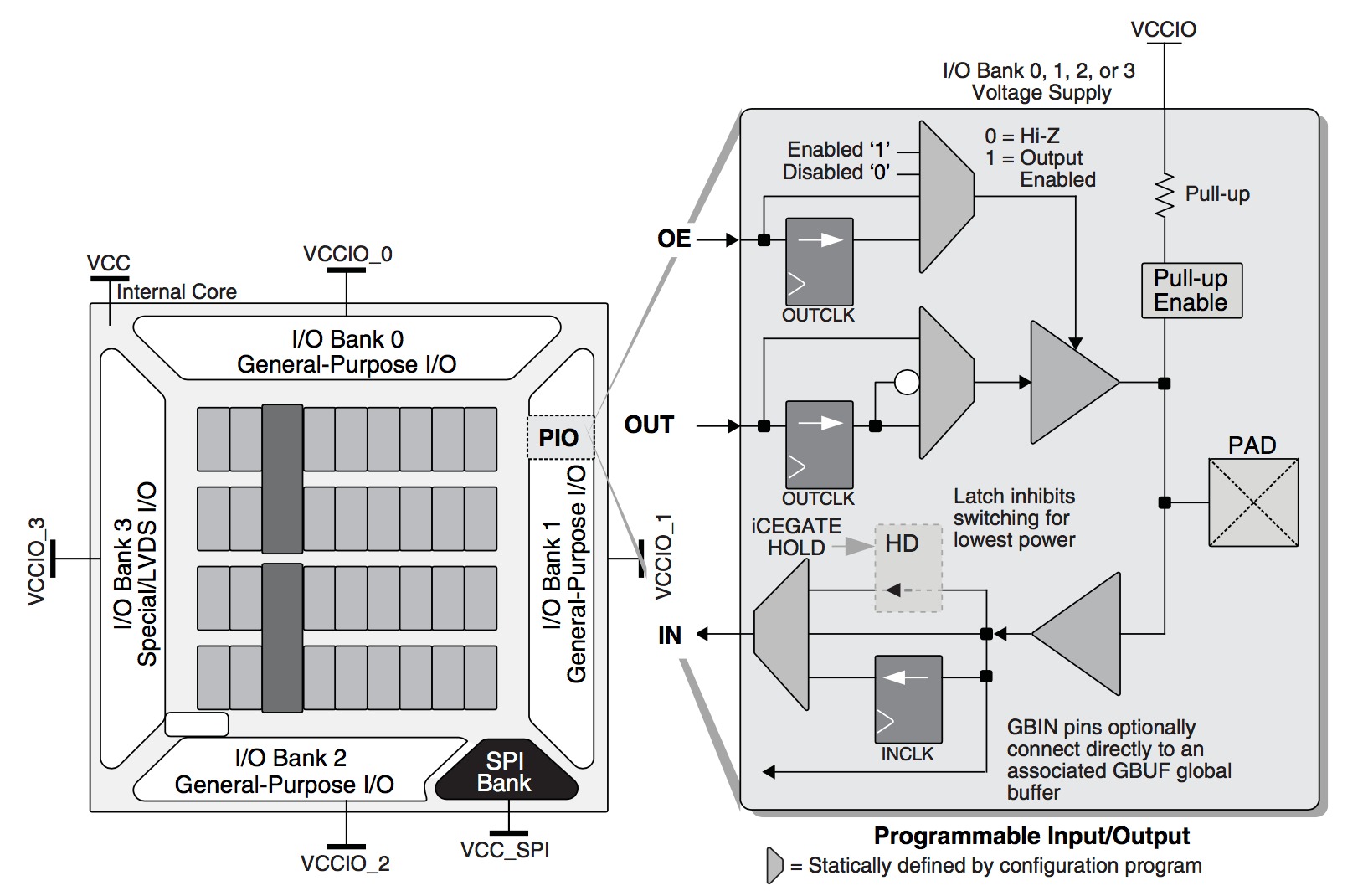
# SB_IO() ::
#    CLOCK_ENABLE:In(Bit),
#    INPUT_CLOCK':In(Bit),
#    OUTPUT_CLOCK':In(Bit),
#    OUTPUT_ENABLE':In(Bit),
#    LATCH_INPUT_VALUE':In(Bit),
#    D_IN_0':In(Bit), # rising
#    D_IN_1':In(Bit), # falling
#    PACKAGE_PIN: InOut(Bit)
#    D_OUT_0':Out(Bit), # rising
#    D_OUT_1':Bit, # falling
#    PACKAGE_PIN: Bit # inout
SB_IO(PIN_TYPE=int6)
This primitive is controlled using the parameter PIN_TYPE.
PLL
A PLL can be created using the following useful function.
# SB_PLL :: I, In(Bit), O, Out(Bit)
SB_PLL( freqout, freqin=12000000 ):
Here, I is the reference clock and O is the new clock signsl.
This function configures the low-level primitive SB_PLL40_CORE.
# SB_PLL40_CORE ::
#            "REFERENCECLK", In(Bit),
#            "RESETB", In(Bit),
#            "BYPASS", In(Bit),
#            "PLLOUTCORE", Out(Bit),
#            "PLLOUTGLOBAL", Out(Bit)